IC BUFF NON-INVERT 5.5V 5-TSSOP
11/6/2025 1:05:14 AM
Nexperia USA Inc. 74LVC1G125GW-Q100
.jpg "74LVC1G125GW-Q100")

- Part No.:
- 74LVC1G125GW-Q100
- Manufacturer:
- Nexperia USA Inc.
- Category:
- Posts
- Datasheet:
-
 74LVC1G125GW-Q100.pdf
- Description:
- IC BUF NON-INVERT 5.5V 5TSSOP
- Quantity:
- RFQ
- Payment:

- Shipping:

 74LVC1G125GW-Q100 details
74LVC1G125GW-Q100 is a single-channel tri-state buffer/line driver launched by Nexperia, specifically designed for automotive electronics. It meets the AEC-Q100 automotive qualification and is suitable for harsh environments such as in-vehicle networks, sensor interfaces, and Body Electronic Control Units (ECUs). Below is a detailed description of its core features and technical specifications:
1. Core Functions and Applications
Key RolesThis device is mainly used for amplifying signal strength, matching logic levels, and isolating circuits. It supports level conversion in 3.3 V to 5 V mixed-voltage systems, especially for signal transmission between in-vehicle sensors (e.g., tire pressure monitoring systems, temperature sensors) and microcontrollers. Its Schmitt trigger input effectively suppresses noise and improves signal stability, making it suitable for high-speed data buses (e.g., CAN, LIN) and low-speed control signal links.
Typical Application Scenarios
In-vehicle infotainment systems (e.g., connections between central control displays and audio modules)
Input/output interfaces of Body Electronic Control Units (ECUs)
Sensor signal conditioning (e.g., converting low-level analog signals to digital logic levels)
Enable control circuits of automotive power management modules
2. Key Technical Parameters
2.1 Electrical Characteristics
Supply Voltage Range: 1.65 V to 5.5 V, compatible with wide voltage fluctuations of 12V in-vehicle systems.
Output Drive Capability: ±32 mA (@VCC=3.3 V), capable of directly driving high loads (e.g., relay coils, LED arrays).
Tri-State Control: The output is in high-impedance state when the enable pin (OE) is at high level, supporting bus sharing and hot-swapping functions.
Logic Level Compatibility: Input is compatible with CMOS/TTL levels, and the output can be configured as push-pull or high-impedance, adapting to various interface protocols.
Power Consumption: Maximum quiescent current (ICC) is only 4 μA, supporting partial power-down mode (IOFF) to prevent damage from reverse current during power-off.
2.2 Signal Integrity
Propagation Delay: Typical value 5-10 ns (@VCC=3.3 V), meeting the requirements of high-speed signal transmission (e.g., communication rates above 100 Mbps).
Input Capacitance: 5 pF (@1 MHz), with minimal impact on high-frequency signals, suitable for buffering clock lines and data lines.
Noise Suppression: Schmitt trigger input can filter ±0.2 V noise, enhancing signal anti-interference capability.
2.3 Physical Characteristics
Package: Ultra-compact TSSOP-5 (SOT-353-1), measuring 2.25 mm × 1.35 mm × 1.00 mm, ideal for high-density PCB layouts.
Pin Configuration: 5 pins (input, output, enable, power supply, ground), facilitating connection of differential signals and ground.
Operating Temperature Range: -40°C to +125°C, meeting automotive environmental requirements.
3. Technical Advantages
High Reliability and ComplianceIt is AEC-Q100 Grade 1 qualified, RoHS and halogen-free compliant, and can withstand more than 1000 thermal cycle tests.
ESD Protection: 2000 V HBM (Human Body Model), 1000 V CDM (Charged Device Model), exceeding industry standards.
Latch-Up Protection: Latch-up current resistance exceeds 250 mA (JESD 78 Class II), ensuring long-term stability.
Design FlexibilityCompatible with various packages such as SOT-23, TSOP-5, and XSON-5, enabling direct replacement of older models without modifying PCB designs.
Supports partial power-down mode, cutting off the output through the IOFF function to avoid leakage current when unpowered.
Cost OptimizationSingle-channel design reduces redundant functions and lowers BOM cost.
Low-power consumption reduces the burden on the in-vehicle power system and extends battery life.
- Package/Case:Surface Mount
- Packaging:Tape & Reel (TR),Cut Tape (CT)
- Series:Automotive, AEC-Q100, 74LVC
- ProductStatus:Active
- LogicType:Buffer, Non-Inverting
- NumberofElements:1
- NumberofBitsperElement:1
- InputType:-
- OutputType:3-State
- Current-OutputHighLow:32mA, 32mA
- Voltage-Supply:1.65V ~ 5.5V
- OperatingTemperature:-40°C ~ 125°C (TA)
- MountingType:
- Category:
- Datasheet:
1.How to find the detailed information of 74LVC1G125GW-Q100 chips/componets? Including Microchip Technology original factory information, 74LVC1G125GW-Q100 pictures, Posts application?
You can use the intelligent search engine of jinftry.com, or filter by Active Filters category, or find it through Microchip Technology page.
2.How does E-BEST INDUSTRIAL (HK) CO.,LTD guarantee that 74LVC1G125GW-Q100 is the original manufacturer or agent of Microchip Technology?
We have a very professional business development department to strictly test and verify the qualifications of Microchip Technology original manufacturers and agents. All Microchip Technology suppliers must pass the qualification review before they can publish their 74LVC1G125GW-Q100 devices; we pay more attention to the channels and quality of 74LVC1G125GW-Q100 products than any other customer. We strictly implement supplier audits, so you can purchase with confidence.
3.Are the 74LVC1G125GW-Q100 price and stock displayed on the platform accurate?
The Microchip Technology's inventory fluctuates greatly and cannot be updated in time, it will be updated periodically within 24 hours. After submitting an order for 74LVC1G125GW-Q100, it is recommended to confirm the order with E-BEST INDUSTRIAL (HK) CO.,LTD salesperson or online customer service before payment.
4.What forms of payment can I use in E-BEST INDUSTRIAL (HK) CO.,LTD?
TT Bank,Wire Transfer, Paypal, Credit Card, Western Union, and Escrow is all acceptable.
5.How is the shipping arranged and track my package?
Customers can choose industry-leading freight companies, including DHL, UPS, FedEx, TNT, and Registered Mail.
Once your order has been processed for shipment, our sales will send you an email advising you of the shipping status and tracking number.
Warm Tips: It may take up to 24 hours before carriers will display tracking information. In normal conditions, Express delivery needs 3-5 days, and Registered Mail needs 25-60 days.
6. What is the process for returns or replacement of 74LVC1G125GW-Q100?
All goods will implement Pre-Shipment Inspection (PSI), selected at random from all batches of your order to do a systematic inspection before arranging the shipment. If there is something wrong with the 74LVC1G125GW-Q100 we delivered, we will accept the replacement or return of the 74LVC1G125GW-Q100 only when all of the below conditions are fulfilled:
(1)Such as a deficiency in quantity, delivery of wrong items, and apparent external defects (breakage and rust, etc.), and we acknowledge such problems.
(2)We are informed of the defect described above within 90 days after the delivery of 74LVC1G125GW-Q100.
(3)The PartNo is unused and only in the original unpacked packaging.
Two processes to return the products:
(1)Inform us within 90 days
(2)Obtain Requesting Return Authorizations
7.How to contact us and get support of technology, such as 74LVC1G125GW-Q100 pin diagram, 74LVC1G125GW-Q100 datasheet pdf?
If you need any After-Sales service, please feel free contact us: candy@ebest-hk.com.
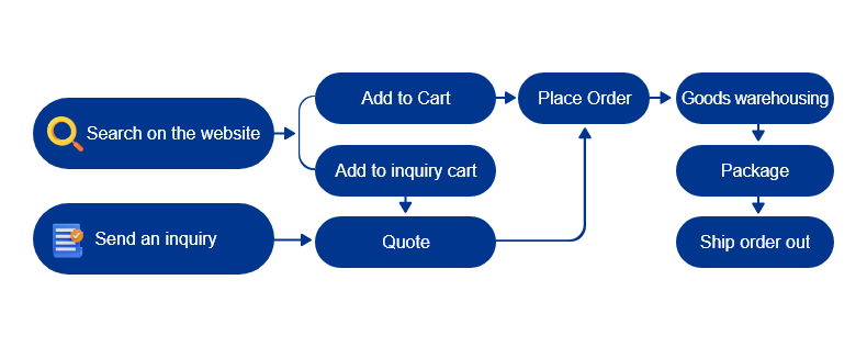
74LVC1G125GW-Q100 Shopping process
2,496 Availability
- Quantity:
- Add To Cart
Please send RFQ.
Warm Tips: Please fill out the below form and we will contact you as soon as possible.
Contact Us
Your dedicated customer service, providing you the best service at any time.
- Telephone
- +86 13510572937
- candy@ebest-hk.com
- Skype
- e-well-cora