XCKU3P-2FFVA676I is a high-performance, low-power FPGA belonging to Xilinx's Kintex UltraScale™ series, fabricated on a 28nm High-K Metal Gate (HKMG) CMOS process. It strikes an optimal balance between logic density, high-speed signal processing capabilities, and power efficiency, targeting mid-to-high-end applications that demand massive parallel computing, high-bandwidth connectivity, and real-time data processing. The device is widely adopted in data centers, industrial automation, 5G communication, test and measurement equipment, and aerospace/defense systems, enabling core functions such as 5G baseband processing, AI/ML acceleration, advanced motor control, high-speed interface bridging, and radar signal processing.
-
Logic Slices: 35,488 (composed of 5,545 Slice Groups, each integrating 6 LUTs and 8 flip-flops), supporting complex combinational and sequential logic implementation for large-scale designs.
-
LUTs (Look-Up Tables): 33,270 (6-input LUTs), configurable as logic gates, distributed RAM (up to 64Kb total), or shift registers for flexible data processing and temporary storage.
-
Flip-Flops: 53,232 (1:1.6 ratio with LUTs), ensuring sufficient sequential logic resources for timing-critical high-speed applications (e.g., clocked logic, state machines).
-
DSP Slices: 288 enhanced DSP48E2 slices (25x17 multiplier accumulators with pre-adder/post-adder), supporting floating-point arithmetic, FFT/IFFT, filtering, and complex signal processing tasks with 2x higher throughput than previous-generation DSP48E1 slices.
-
Embedded Memory: 10.3 Mb (distributed as 258 Block RAMs, each 36Kb), configurable as dual-port RAM, single-port RAM, ROM, FIFO, or shift registers with ECC (Error Correction Code) support for critical data integrity.
-
Clock Management Tiles (CMTs): 6, each integrating 1 PLL and 2 Mixed-Mode Clock Managers (MMCMs) for precise clock synthesis, jitter reduction, and frequency tuning up to 1.0 GHz.
-
Global Clock Networks: 32 low-skew global clock lines, ensuring stable clock distribution across the entire device with minimal timing deviation.
-
GTX Transceivers: 24 integrated GTX transceivers, supporting data rates up to 12.5 Gbps (line rate) for high-speed serial communication.
-
Supported Serial Protocols: PCI Express Gen3 (x16), 10G/25G Ethernet, CPRI/OBSAI (up to 10.1376 Gbps), SATA III, XAUI, JESD204B (for high-speed data converters), and custom high-speed interfaces.
-
Total I/O Pins: 460 (including general-purpose I/Os and dedicated interface pins), enabling high-density peripheral integration for complex systems.
-
I/O Standards: Compatible with LVTTL, LVCMOS (1.2V/1.5V/1.8V/2.5V/3.3V), SSTL, HSTL, LVDS, and Differential Signaling Levels (DSL), supporting mixed-voltage system integration.
-
I/O Banks: 10 independent I/O banks with configurable voltage domains (1.2V~3.3V), providing flexibility for connecting to diverse peripherals (sensors, ADCs/DACs, memory modules).
-
Package Type: FFVA676 (676-pin Fine-Pitch Ball Grid Array, FPBGA), 27mm×27mm body size, 1.0mm ball pitch, offering high pin density and excellent thermal conductivity.
-
Mounting Method: Surface Mount Technology (SMT), compatible with lead-free reflow soldering (peak temperature ≤260℃, complying with IPC/JEDEC standards).
-
Weight: Approximately 15g (typical), suitable for high-density PCB layouts and rugged industrial/aerospace applications.
-
Supply Voltage: Core voltage (VCCINT) 0.9V; I/O voltage (VCCIO) 1.2V/1.5V/1.8V/2.5V/3.3V; auxiliary voltage (VCCAUX) 1.8V; transceiver voltage (VCCGTX) 1.0V/1.8V.
-
Maximum Operating Frequency: Up to 500 MHz (combinational logic), 400 MHz (sequential logic), and 12.5 Gbps (serial transceivers).
-
Operating Temperature Range: Industrial grade (-40℃~+125℃), adapting to harsh environments such as industrial workshops, outdoor communication towers, and aerospace systems.
-
Power Consumption: Typical static power 3.1W, dynamic power 12.5W (at 100 MHz logic operation + 8x GTX transceivers @ 6.25 Gbps), optimized for performance-power balance.
-
Configuration Options: JTAG (IEEE 1149.1), Serial Flash (SPI), BPI Flash, and SelectMAP, supporting in-system reconfiguration (ISR) and secure configuration with bitstream encryption (AES-256) and authentication (HMAC-SHA256).
The part number XCKU3P-2FFVA676I follows Xilinx's Kintex UltraScale naming convention, with each segment indicating key attributes:
-
XCKU: Series identifier (Kintex UltraScale™ family).
-
3P: Logic density grade (3P denotes the mid-range variant with balanced logic, DSP, and memory resources).
-
2: Speed grade (standard speed; higher numbers indicate faster performance with lower propagation delay).
-
FFVA676: Package code (676-pin Fine-Pitch Ball Grid Array, FPBGA).
-
I: Temperature grade (industrial grade, -40℃~+125℃).
Adopts 28nm HKMG process technology, delivering 40% higher performance and 50% lower power consumption compared to previous-generation 40nm FPGAs. The optimized Slice Group structure and DSP48E2 slices enable efficient implementation of compute-intensive algorithms with reduced latency and power dissipation.
24 GTX transceivers support multi-gigabit serial communication up to 12.5 Gbps, eliminating the need for external transceivers and reducing system complexity. Native support for industry-standard protocols (e.g., PCIe Gen3, 10G/25G Ethernet, JESD204B) ensures seamless integration with high-speed peripherals and networks.
288 DSP48E2 slices support single-cycle multiply-accumulate (MAC) operations, floating-point arithmetic, and complex signal processing tasks (e.g., beamforming, radar signal processing, AI inference acceleration). The enhanced DSP architecture provides higher throughput and flexibility for diverse computational workloads.
35k+ logic slices and 10.3 Mb embedded memory offer sufficient capacity for large-scale logic designs and data buffering. The 36Kb Block RAMs support dual-port operation and ECC, making them ideal for critical data storage in industrial, aerospace, and medical applications.
Supports secure boot with bitstream encryption (AES-256) and authentication (HMAC-SHA256), protecting intellectual property (IP) from tampering and unauthorized access. Industrial-grade temperature range (-40℃~+125℃) and robust mechanical design ensure stable operation in harsh environments with high shock, vibration, and temperature fluctuations.
Fully compatible with Xilinx's Vivado Design Suite, supporting Verilog, VHDL, and SystemVerilog design entry. Xilinx's comprehensive IP core library (e.g., FFT, Ethernet, PCIe, JESD204B, AI Engine) accelerates design cycles, while the UltraScale Architecture's hierarchical clocking and routing optimize timing closure for high-speed designs.
-
High-speed network interface cards (NICs) and switches (10G/25G Ethernet).
-
AI/ML acceleration for edge computing nodes and cloud servers (lightweight neural network inference).
-
Storage area network (SAN) controllers (SATA III, NVMe over PCIe).
-
High-performance Programmable Logic Controllers (PLCs) and motion controllers for multi-axis synchronization.
-
Industrial Ethernet gateways (Profinet, Ethernet/IP, Modbus TCP) with 10Gbps support.
-
Machine vision systems (high-resolution image processing, pattern recognition, real-time analytics).
-
Servo drives and motor control systems (high-precision torque control and position feedback).
-
5G base stations and small cells (baseband processing, beamforming, signal modulation).
-
Optical transceivers and network switches (10G/25G Ethernet, CPRI/OBSAI).
-
IoT gateways and edge computing nodes (high-speed data aggregation and processing).
-
High-speed oscilloscopes and signal generators (data acquisition, waveform synthesis).
-
Protocol analyzers (PCIe, Ethernet, JESD204B) and automated test equipment (ATE).
-
Radar and lidar test systems (signal simulation, data analysis, target emulation).
-
Radar and sonar signal processing (target detection, tracking, classification).
-
Satellite communication terminals (modulation/demodulation, data framing, encryption).
-
Avionics systems (flight control, navigation, in-flight entertainment).
1.How to find the detailed information of XCKU3P-2FFVA676I chips/componets? Including Microchip Technology original factory information, XCKU3P-2FFVA676I pictures, Posts application?
You can use the intelligent search engine of jinftry.com, or filter by Active Filters category, or find it through Microchip Technology page.
2.How does E-BEST INDUSTRIAL (HK) CO.,LTD guarantee that XCKU3P-2FFVA676I is the original manufacturer or agent of Microchip Technology?
We have a very professional business development department to strictly test and verify the qualifications of Microchip Technology original manufacturers and agents. All Microchip Technology suppliers must pass the qualification review before they can publish their XCKU3P-2FFVA676I devices; we pay more attention to the channels and quality of XCKU3P-2FFVA676I products than any other customer. We strictly implement supplier audits, so you can purchase with confidence.
3.Are the XCKU3P-2FFVA676I price and stock displayed on the platform accurate?
The Microchip Technology's inventory fluctuates greatly and cannot be updated in time, it will be updated periodically within 24 hours. After submitting an order for XCKU3P-2FFVA676I, it is recommended to confirm the order with E-BEST INDUSTRIAL (HK) CO.,LTD salesperson or online customer service before payment.
4.What forms of payment can I use in E-BEST INDUSTRIAL (HK) CO.,LTD?
TT Bank,Wire Transfer, Paypal, Credit Card, Western Union, and Escrow is all acceptable.
5.How is the shipping arranged and track my package?
Customers can choose industry-leading freight companies, including DHL, UPS, FedEx, TNT, and Registered Mail.
Once your order has been processed for shipment, our sales will send you an email advising you of the shipping status and tracking number.
Warm Tips: It may take up to 24 hours before carriers will display tracking information. In normal conditions, Express delivery needs 3-5 days, and Registered Mail needs 25-60 days.
6. What is the process for returns or replacement of XCKU3P-2FFVA676I?
All goods will implement Pre-Shipment Inspection (PSI), selected at random from all batches of your order to do a systematic inspection before arranging the shipment. If there is something wrong with the XCKU3P-2FFVA676I we delivered, we will accept the replacement or return of the XCKU3P-2FFVA676I only when all of the below conditions are fulfilled:
(1)Such as a deficiency in quantity, delivery of wrong items, and apparent external defects (breakage and rust, etc.), and we acknowledge such problems.
(2)We are informed of the defect described above within 90 days after the delivery of XCKU3P-2FFVA676I.
(3)The PartNo is unused and only in the original unpacked packaging.
Two processes to return the products:
(1)Inform us within 90 days
(2)Obtain Requesting Return Authorizations
7.How to contact us and get support of technology, such as XCKU3P-2FFVA676I pin diagram, XCKU3P-2FFVA676I datasheet pdf?
If you need any After-Sales service, please feel free contact us: candy@ebest-hk.com.
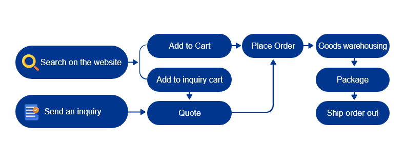
XCKU3P-2FFVA676I Shopping process


 XCKU3P-2FFVA676I.pdf


 XCKU3P-2FFVA676I details