LTC2262IUJ-14 is a 14-bit high-precision high-speed Analog-to-Digital Converter (ADC) launched by ADI (Analog Devices, formerly Linear Technology). Designed based on an advanced pipelined architecture, it integrates a differential input buffer, internal reference, and SPI configuration interface, fully compliant with industrial-grade reliability standards. Specifically built for scenarios requiring strict sampling rate, linearity, and low power consumption-such as communication systems, instrumentation, Data Acquisition Systems (DAQ), radio frequency receivers, and medical devices-it is a cost-effective high-speed analog signal digitization solution.
-
Product Category: 14-bit high-speed pipelined ADC (Analog-to-Digital Converter), a high-performance mixed-signal device
-
Brand: ADI (Analog Devices), formerly Linear Technology-a global leader in high-performance analog and power management solutions
-
Core Electrical Parameters:
-
Resolution: 14-bit (no missing codes, DNL ±0.5LSB, INL ±2LSB typical)
-
Sampling Rate: Up to 125MSps (Mega Samples per Second), meeting mid-to-high frequency signal sampling needs
-
Input Characteristics: Differential analog input, input voltage range ±0.5Vpp~±2Vpp (configurable via external resistors), input bandwidth ≥700MHz, supporting wideband signal sampling
-
Output Interface: LVDS (Low-Voltage Differential Signaling) parallel output, compatible with CMOS logic levels, supporting data interleaving mode to reduce transmission noise
-
Reference Voltage: Built-in 2.5V high-precision reference (temperature coefficient ±10ppm/℃); external reference (2.0V~3.0V) also supported for flexible precision adaptation
-
Operating Conditions:
-
Supply Voltage: Dual-supply operation (1.8V for analog section, 1.8V/3.3V compatible for digital section); external voltage division required for single-supply mode
-
Operating Temperature Range: Industrial grade (-40℃~85℃), adapting to harsh environment applications
-
Power Consumption: 195mW typical (125MSps sampling rate, dual 1.8V supply), standby power consumption <1mW, featuring significant low-power characteristics
-
Package Type: 48-lead QFN (Quad Flat No-Lead) package (7mm×7mm), lead-free design, surface-mount, suitable for high-density PCB layouts
-
Product Status: Active (in mass production) with a stable supply chain. As a classic model in ADI's high-speed ADC series, it is widely used in communication and test & measurement fields
-
Core Advantages: Balances 14-bit high precision and 125MSps high-speed sampling; wide input bandwidth adapts to multi-frequency signals; LVDS output offers strong anti-interference; low power consumption and industrial-grade temperature range suit multiple scenarios
-
Core Architecture: Adopts pipelined ADC topology, combined with high-speed comparators and digital error correction logic, balancing sampling rate and linearity. No missing codes guarantee full-range sampling accuracy
-
Integrated Functions: Single-chip integration of 14-bit ADC core, differential input buffer amplifier, built-in reference voltage source, LVDS output driver, and SPI configuration circuit. Only external clock, decoupling capacitors, and a few configuration resistors are required to form a complete sampling solution, simplifying hardware design
-
Clock and Trigger: Supports differential/single-ended sampling clock input; Duty Cycle Stabilizer (DCS) ensures sampling precision over a wide duty cycle range; supports external trigger and continuous sampling mode switching
-
Configuration Interface: 3-wire SPI serial interface for configuring input range, reference mode, output format, and other parameters; supports register power-down retention, eliminating the need for reconfiguration
-
Precision Indicators (typical values, fS=125MSps, VREF=2.5V, TA=25℃):
-
Differential Nonlinearity (DNL): ±0.3LSB, no missing codes, ensuring uniform sampling steps
-
Integral Nonlinearity (INL): ±1.5LSB, guaranteeing linear restoration of sampled signals
-
Signal-to-Noise Ratio (SNR): 74dB (1kHz input signal, at Nyquist frequency); Spurious-Free Dynamic Range (SFDR): 90dBc, low-noise characteristics adapt to weak signal sampling
-
Total Harmonic Distortion (THD): -80dBc, minimal harmonic interference, high signal restoration
-
Dynamic Performance:
-
Input Bandwidth: ≥700MHz, supporting direct sampling of Radio Frequency (RF) and Intermediate Frequency (IF) signals without additional down-conversion circuits
-
Sample-and-Hold Time: 6ns, ensuring signal hold stability during high-speed sampling
-
Clock Jitter Tolerance: <50fs (femtoseconds), reducing the impact of clock noise on sampling precision
-
Reference Characteristics: Built-in reference output noise ≤50μVrms (1kHz bandwidth); external reference input impedance is high (10kΩ), minimizing impact on external circuit loads
-
Power Consumption Optimization Design (typical values):
-
Active Power Consumption: 195mW (125MSps, dual 1.8V supply), 210mW (125MSps, analog 1.8V + digital 3.3V)
-
Standby Power Consumption: <1mW, significantly reducing energy consumption in idle state
-
Adaptive Power Adjustment with Sampling Rate: When sampling rate drops to 62.5MSps, power consumption can be as low as 110mW, adapting to different rate requirements
-
Reliability Assurance:
-
ESD Protection Level: ±2kV (HBM), ±200V (MM), compliant with IEC 61000-4-2 standard, enhancing anti-static interference capability
-
Long-Term Stability: Reference voltage annual drift <50ppm, ensuring long-term operational precision of equipment
-
Pin Protection: Analog input pins feature overvoltage protection (±5V) to prevent chip damage from misoperation
-
Compliance: Compliant with RoHS 2.0 and REACH environmental standards, meeting global market compliance requirements
-
Input Configuration: Supports single-ended to differential input (requires external resistor network); differential input mode offers strong common-mode interference rejection, adapting to high-noise industrial field environments
-
Output Configuration: LVDS output supports 1.8V/3.3V logic levels; data format selectable between two's complement or offset binary; supports data alignment and delay adjustment
-
Calibration Function: Supports self-calibration and system calibration, triggered via SPI commands, automatically compensating for gain and offset errors to improve system precision
-
Power Supply Rejection Ratio (PSRR): 60dB (1kHz) for analog section, 50dB (1kHz) for digital section, strong suppression capability against power supply noise, reducing the impact of power fluctuations
-
125MSps sampling rate combined with 700MHz input bandwidth enables direct sampling of Intermediate Frequency (IF) and Radio Frequency (RF) signals, eliminating the need for down-conversion circuits in traditional solutions and simplifying system architecture
-
14-bit resolution + 74dB SNR + 90dBc SFDR delivers excellent sampling precision, accurately restoring weak signals and complex waveforms, meeting high-precision requirements of test & measurement and communication reception scenarios
-
Dual-supply/single-supply compatible design; 195mW low power consumption (125MSps) is 20% lower than comparable ADCs, extending battery life of battery-powered devices
-
Adaptive power adjustment with sampling rate, flexibly configurable between 5MSps~125MSps according to actual needs, balancing performance and energy consumption
-
Built-in high-precision reference, input buffer, and LVDS output driver reduce the number of external components, lowering BOM costs and PCB space
-
SPI configuration interface supports register-level customization; LVDS differential output offers strong anti-interference and long transmission distance, adapting to high-speed signal transmission scenarios
-
-40℃~85℃ industrial-grade wide temperature range tolerates extreme high and low temperature environments, adapting to harsh scenarios such as industrial control and automotive communication (non-safety-related)
-
Enhanced ESD protection and overvoltage protection provide strong Electromagnetic Interference (EMI) resistance, reducing failure risks in harsh environments
-
Communication Systems: 5G small base stations, radio frequency receivers, Software Defined Radio (SDR), satellite communication equipment, supporting direct intermediate frequency signal sampling
-
Instrumentation: Digital oscilloscopes, spectrum analyzers, signal generators, high-speed data recorders, meeting wideband high-precision measurement needs
-
Data Acquisition Systems (DAQ): Industrial automation data acquisition, seismic monitoring equipment, ultrasonic testing systems, adapting to high-speed multi-channel sampling
-
Medical Devices: Ultrasound imagers, portable diagnostic equipment, low-power and high-precision characteristics meet medical scenario requirements
-
Aerospace and Defense: Radar signal processing, electronic countermeasure equipment, wide temperature range and high reliability adapt to extreme environments
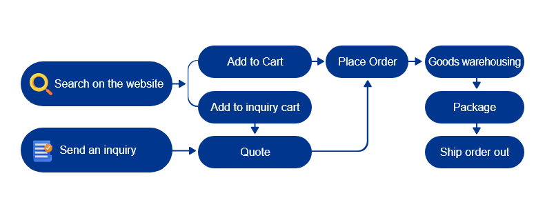
1.How to find the detailed information of LTC2262IUJ-14 chips/componets? Including Microchip Technology original factory information, LTC2262IUJ-14 pictures, Posts application?
You can use the intelligent search engine of jinftry.com, or filter by Active Filters category, or find it through Microchip Technology page.
2.How does E-BEST INDUSTRIAL (HK) CO.,LTD guarantee that LTC2262IUJ-14 is the original manufacturer or agent of Microchip Technology?
We have a very professional business development department to strictly test and verify the qualifications of Microchip Technology original manufacturers and agents. All Microchip Technology suppliers must pass the qualification review before they can publish their LTC2262IUJ-14 devices; we pay more attention to the channels and quality of LTC2262IUJ-14 products than any other customer. We strictly implement supplier audits, so you can purchase with confidence.
3.Are the LTC2262IUJ-14 price and stock displayed on the platform accurate?
The Microchip Technology's inventory fluctuates greatly and cannot be updated in time, it will be updated periodically within 24 hours. After submitting an order for LTC2262IUJ-14, it is recommended to confirm the order with E-BEST INDUSTRIAL (HK) CO.,LTD salesperson or online customer service before payment.
4.What forms of payment can I use in E-BEST INDUSTRIAL (HK) CO.,LTD?
TT Bank,Wire Transfer, Paypal, Credit Card, Western Union, and Escrow is all acceptable.
5.How is the shipping arranged and track my package?
Customers can choose industry-leading freight companies, including DHL, UPS, FedEx, TNT, and Registered Mail.
Once your order has been processed for shipment, our sales will send you an email advising you of the shipping status and tracking number.
Warm Tips: It may take up to 24 hours before carriers will display tracking information. In normal conditions, Express delivery needs 3-5 days, and Registered Mail needs 25-60 days.
6. What is the process for returns or replacement of LTC2262IUJ-14?
All goods will implement Pre-Shipment Inspection (PSI), selected at random from all batches of your order to do a systematic inspection before arranging the shipment. If there is something wrong with the LTC2262IUJ-14 we delivered, we will accept the replacement or return of the LTC2262IUJ-14 only when all of the below conditions are fulfilled:
(1)Such as a deficiency in quantity, delivery of wrong items, and apparent external defects (breakage and rust, etc.), and we acknowledge such problems.
(2)We are informed of the defect described above within 90 days after the delivery of LTC2262IUJ-14.
(3)The PartNo is unused and only in the original unpacked packaging.
Two processes to return the products:
(1)Inform us within 90 days
(2)Obtain Requesting Return Authorizations
7.How to contact us and get support of technology, such as LTC2262IUJ-14 pin diagram, LTC2262IUJ-14 datasheet pdf?
If you need any After-Sales service, please feel free contact us: candy@ebest-hk.com.


 LTC2262IUJ-14.pdf

 LTC2262IUJ-14 details