Methods for measuring the temperature of semiconductor devices
Despite groundbreaking advancements in the field of semiconductors, the main issue that chipmakers are dealing with is the overheating of these devices. This problem reduces their overall efficiency and shell life, adding more cost and consumption of limited resources. To tackle this issue, innovations and methods are being developed to detect this overheating and keep the semiconductor at its operational temperature.
The operational temperature dramatically impacts the performance and reliability of semiconductor devices, as the temperature is the most commonly measured environmental variable. This is justified as electrical, mechanical, chemical, and biological systems are altered by temperature. Therefore, we need temperature measuring methods that will provide input to a controlling unit, maintaining the system's operational temperature conditions.
It is safe to assume that the uprating of a semiconductor device decreases as temperature increases. For instance, the transconductance of a transistor may differ concerning increasing temperature (depending on the device configuration and working conditions). Figure 1 shows the relationship between the uprating of a semiconductor and its temperature.
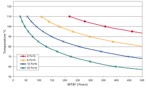
Fig 1 Uprating vs temperature
Therefore, this article explains different methods with their parameters to measure the temperature of semiconductor devices and shares an insight into accuracy and spatial and temporal resolution. It is noteworthy that the majority of temperature measurement challenges include the improvement of these quantities.
Ⅰ. Methods to measure the temperature of a semiconductor device
Generally, there are three approaches to measuring the temperature of a semiconductor device. These approaches include an optical method, a physically contacting method, and an electrical method, each of which has its own set of advantages and disadvantages.
A) Optical Method: The temperature is measured by using optical properties such as luminescence, reflected radiation, naturally emitted radiation, or forced emitted radiation. For instance, consider that a concentrated beam of photons is focused at a point on the device. A part of this beam of photons may be reflected back due to the change in temperature of the device as diffusion in the energy of the lattice photons is a function of the temperature.
Therefore, we can simply measure the variation in photon-photon interaction and infer the change in temperature of the probed object(thermometer) which lies in the region of the incident beam of photons.
This method can measure the temperature of a body with very high spatial resolution and requires no contact. Furthermore, it can also measure rapid changes in temperature as the time response delay is very less. However, this approach is expensive and requires the target body to be visible.
Ⅱ. Understanding how different optical properties affect temperature
As discussed above, there are different optical properties that dramatically impact the temperature of a semiconductor device. Each of these properties depends on the spectrum of light to detect temperature.
● Luminescence: Luminescence is the emission of radiation as a result of an external stimulus, such as an electromagnetic current or excitation of photons. The emitted radiation is induced by electron and hole reunification, with the peak energy occurring at the band gap energy indirect band gap materials.
Equation 1
The above equation shows that the band gap energy Eg is directly proportional to the square of temperature.
● Infrared Radiation: Infrared radiation is one of the most commonly used optical techniques for measuring temperature. The Stefan-Boltzmann equation for the total emitted energy, which signifies the relation between spectral emittance and temperature is given as

Equation 2
Where ɛ is the emissivity which ranges between 0 to 1 for real emitters. Thus, by using this equation we can determine the temperature of a body by measuring the total emitted radiation. However, the major issue with infrared radiation is the emissivity, as it changes from material to material, thereby causing the overall spectral emittance to vary. Therefore it is important to consider these variations when accounting for temperature.
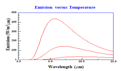
Figure 2 shows how the emission from a semiconductor device varies with temperature.
B) Physically Contacting Method: To begin with, this methodology relies on actual physical contact between the device and the probing object which is usually the thermometer. This approach incorporates point contacting using thermocouples or/and multiple coatings using thermographic phosphorus and liquid crystals. In short, we find that the transfer of thermal energy per unit time from one device to another is the prime factor affecting the measurement of temperature.
The main advantage of this method is that it has a very high spatial resolution and can easily generate temperature maps. However, it requires a physically accessible surface area of the device for contact due to which, the temperature of packaged chips cannot be measured. Moreover, the thermal response is completely dependent upon the response of the probe(thermometer).
Ⅲ. Different Probing devices used to detect the transfer of thermal energy from one device to another
Probing devices play an important role in the Physically Contacting Method as they are present on the body of the device and measure temperature directly.
● Scanning Thermal Probes: These are effectively the only thermal probes that can measure the temperature of a body on a nanoscale. These atomic force microscopes are coupled with temperature-sensitive elements like thermistors or thermocouples to measure temperature.
These probes provide the highest spatial resolution due to their minuscule size. Figure 3 shows different microscopic surfaces and how a thermal probe is placed to detect temperature.
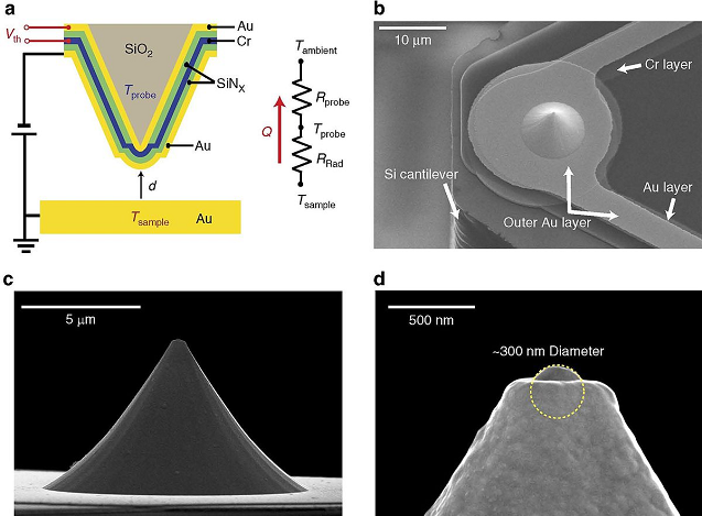
Fig 3 Different probing angles
● Thermographic phosphors: This material is a ceramic powder of phosphor compounds that is doped with rare earth elements which illuminate when exposed to ultraviolet radiation. The intensity of this illumination is temperature-dependent, which decreases as the temperature rises.
C) Electrical Method: Electrical method uses electrical parameters such as PN-Junction forward voltage, threshold voltage, electrical resistance, and current gain. As these parameters vary with temperature, we can easily calculate the temperature of the device. This method provides a lumped average value of the actual temperature distribution. Figure 4 shows the difference in temperature distribution between actual and ideal bodies
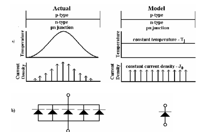
Fig 4 Temperature distribution in actual and real bodies
This method does not require physical contact with the device. However it cannot provide a temperature map as it indicates the temperature for a specific area, for example, the junction temperature is the same only for the junction area and nowhere else. Furthermore, this method requires calibration before temperature measurement.
Ⅳ. Reviewing different electrical parameters which greatly impact temperature measurement
● PN-Junction Forward Voltage: The forward voltage of a PN-Junction is one of the most commonly used parameters for measuring the temperature of a semiconductor device. Figure 5 shows the variation of junction voltage with respect to temperature.
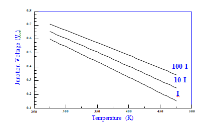
Fig 5: Junction voltage vs Temperature
The relationship between temperature and forward voltage is given by:
Equation 3
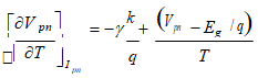
Here, Ipn is the current flowing through the grid having an electron charge q of 1.6·10-19 C, with k as Boltzmann's constant, Eg being the energy band gap of silicon, and Vpn forward voltage. The left-hand side of the equation is approximately -2 mV/K and ranges by about 7 % between 275 K and 475 K. It is also known as the "calibration constant".
● Threshold Voltage: This is another similar electrical parameter used to measure the temperature of a semiconductor device. Figures 6(A) and 6(B) shows the relationship between temperature variation of threshold voltage and temperature derivative of threshold voltage for power MOSFET and integrated circuit MOSFET respectively.
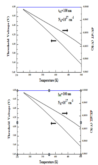
Fig 6 A & B Threshold voltage vs Temperature
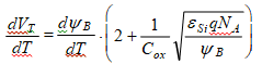
Equation 4
Here VT is the threshold voltage, ψB is the distance from mid gap to fermi level, ε si is the dielectric constant of silicon, COX is the intrinsic gate-channel oxide capacitance and NA is the density of doping. This equation gives us the relationship between threshold voltage and temperature.
Ⅴ. Conclusion
It could be briefly concluded that there are several methods to measure the temperature of a semiconductor device, having their own strengths and weaknesses. Engineers may choose a particular method of measurement based on specific needs such as the requirement of temperature maps, availability of packaged or unpackaged chips, or level of spatial and temporal resolution.
Recommended News


General Inquiry


231,921+
Product Quantity

5,000+
Brands Under Management

16+
Years in Business

220+
Countries & Regions Covered